2D Semiconductor Heterostructures for Optoelectronic Applications
Escarra Photonic Devices and Materials Lab
Our group explores novel materials at the nanoscale and their interactions with light. Two-dimensional materials lie at the forefront of new semiconductor technology, and they have the potential to make electronics smaller, more flexible, and better than previously thought.
A key emphasis in the research in the Escarra Lab has been on studying photovoltaics (solar cells) and optoelectronics from 2-D semiconductors. Before such materials can be used for cutting-edge innovations, such as photovoltaics for power systems of satellites, their synthesis methods and characteristics must be studied and optimized. These materials face challenges in their synthesis, as many aspects of the process can determine the quality of a sample. Many decisions go into designing a particular device from these layered materials, such as bandgaps of different materials, choice of metal contacts, and lattice-matching of the necessary substrate.
I work with a design using multiple different 2-D semiconductor materials, such as MoS2 and ReS2. These materials are two-dimensional direct-bandgap semiconductors that demonstrate unique optoelectronic properties. The materials have shown great promise in fabricating photovoltaics, photodetectors, and light emitters. By working with and analyzing this design, we will be able to demonstrate the potential application of these novel materials in semiconductor technology.
To reach the Escarra Group Website, follow this link.

MoS2 and ReS2
MoS2 is a widely explored and researched 2D semiconductor, with many potential applications for transistors, photodetectors, light emitters, and photovoltaics.
Unique qualities in its monolayer form, having a direct bandgap instead of an indirect bandgap
Exhibits photoluminescence in its 2D form
A naturally n-type material
Grown using Chemical Vapor Deposition (CVD) on sapphire
ReS2 is a less explored 2D semiconductor, with a smaller bandgap than MoS2
Also has a direct bandgap in its monolayer form, as well as a low multilayer form
Also grown using CVD on sapphire
By stacking MoS2 and ReS2, we can create a Type 1 heterostructure device:
The smaller bandgap material (ReS2) sits inside of the larger bandgap (MoS2)
Electrons and holes get confined in the smaller bandgap, and recombine, potentially resulting in high light emission
Device Design and Transfer
We will be creating a lateral heterostructure by stacking MoS2 and ReS2
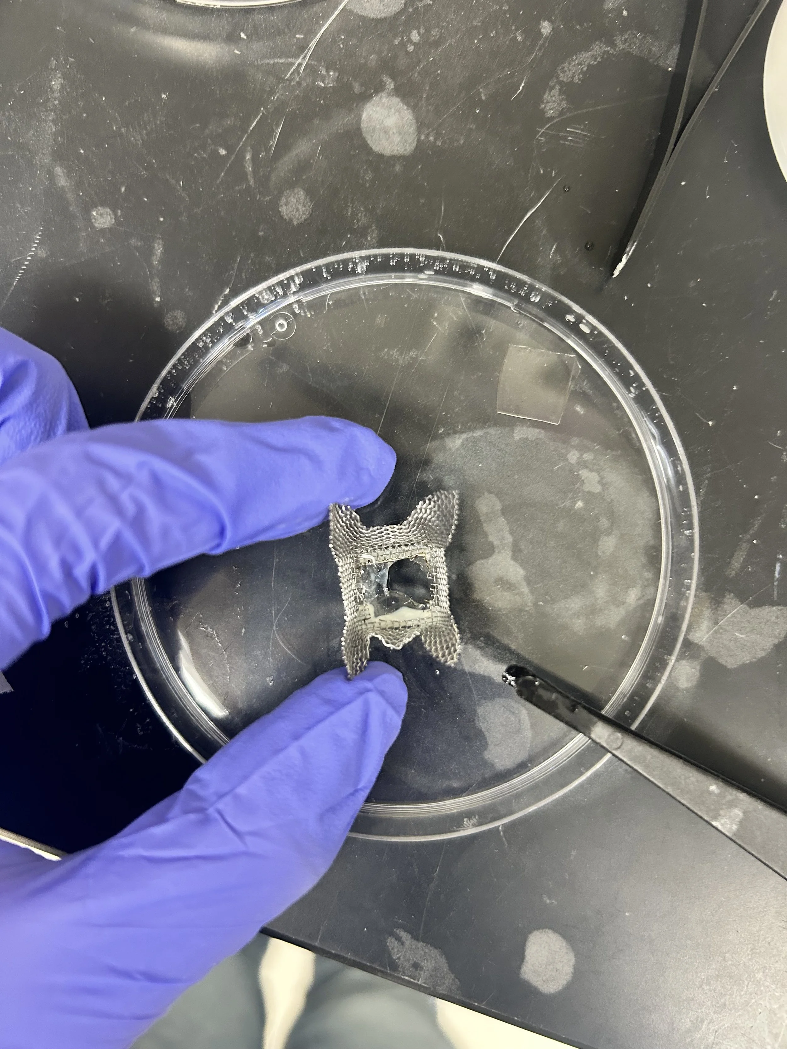
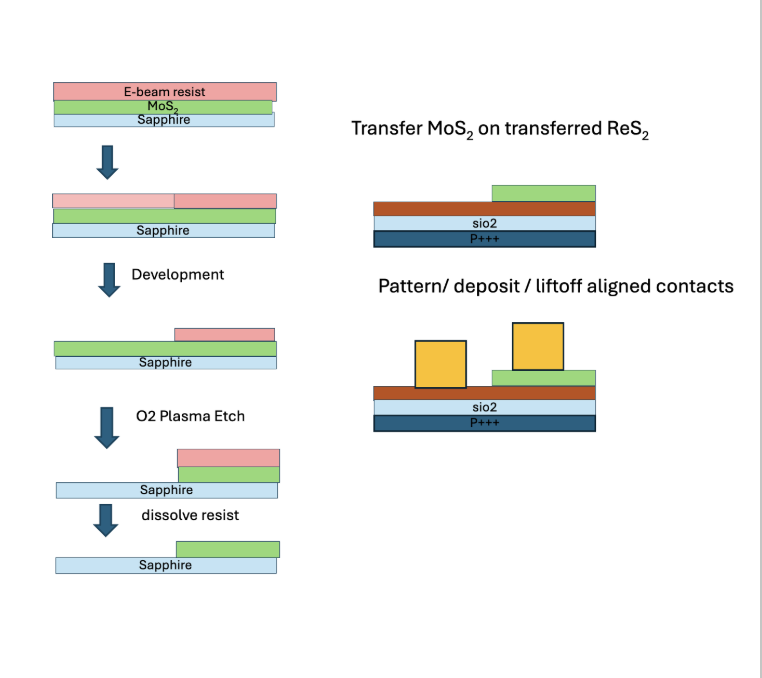
Using our transfer method, we will transfer ReS2 (dark orange) from its sapphire donor to SiO2, due to its ability to create backgating.
We will then etch a sample of MoS2, then align and transfer the MoS2 onto the Res2.
Using EBL, we will pattern metal contacts along the line.
We apply a voltage difference to the metal contacts, injecting electrons and holes
This creates a forward bias, so electrons and holes fall into the lower/higher part of the energy band, where they can then recombine.
After building and testing this device, we can determine if this heterostructure will be a potential photodetector or even light emitter.
Current Work
As of Fall 2025, I am finishing up the work done by the Master’s student who started this project last year. We are in a place where we should hopefully be able to publish a paper by Spring 2026!
My specific and current work on this project includes:
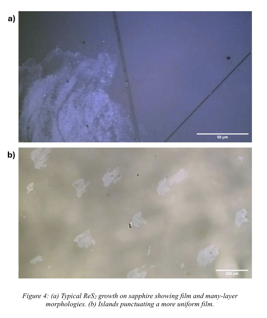
Continuing to grow ReS2 with CVD and see if there is anywhere the process can be improved.
Working on applying the MoS2 transfer process to ReS2 so that we can put it on SiO2.
Designing an alignment mechanism so that we can align the etched MoS2 with the ReS2 sample.